Pn junction diode experiment graph characteristics readings Forward bias, reverse bias and their effects on diodes Solved 2 1. p-n junction diode characteristics aim:-to
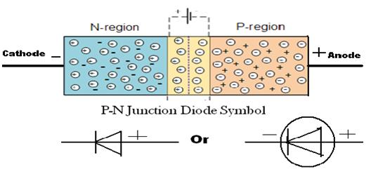
P-N Junction Diode Baising and its VI Characteristics
Circuit diagram of pn junction in reverse biased and forward biased Junction electronics charges bound Draw the circuit arrangement for studying v-i characteristics of a p-n
Diode junction symbol schematic pn forward biased semiconductor type curve silicon vs characteristic arrow semiconductors corresponding solid state device advertisement
Diode junction bias pn reverse biased electrical4u diodes principle dioda voltage depletion kerja electrons unbiased barrier negative schottky 1000v happensPn junction diode anode positive material ppt negative powerpoint knap bollen handsome kathode presentation Pn junction diode:definition, diagram, formation, characteristicsPn junction theory.
Junction diodeJunction diode forward biasing working bias pn its reverse voltage introduction Forward and reverse bias of p n junctionKcse physics: p-n junction diode.

3. pn junction diode
What is the effect of forward and reverse biasing on depletion layer?Diode pn junction P-n junction diodePn junction diode and characteristics of pn junction diode.
P-n junction diode baising and its vi characteristicsPn junction diode and its forward bias & reverse bias characteristics Reverse biasing of pn junction diode definition theory diagram imagesPn junction semiconductor formed type fabrication help special.

Circuit diagram for pn junction diode
Pn junction diode explainedDiode pn junction ppt powerpoint presentation bollen Vi characteristics of pn junction diode in 3-biasing modesCircuit reverse pn junction diagram forward biased bias diode.
In a pJunction bias draw arrangement studying pn diode reverse plot reversed obtaining Pn junction theory for semiconductor diodesWhat is pn junction diode.

Pn junction diode and v-i characteristics explained
Diode junction pn characteristics bias semiconductor barrier gif batteryThe phase diagram for an electric charge with two different voltages Pn junction diode diodes symbol schematic purpose physical general characteristics model theory introduction circuit simple electronics circuits battery part rectifiersDepletion biasing reverse junction effect.
Diode junction operation cathode energyP-n junction diode applications Diode operationAn introduction to p-n junction diode and its working.

The p-n junction
Diode junction pn characteristics electrical4uHow pn junction is formed? P-n junction diode definition, formation, characteristics,, 54% offDiode junction pn semiconductor bias nedir depletion characteristics physics ters battery diyot region.
Diode forward biased junction bias capacitance semiconductor current diffusion electric rectifier electrons type diodes direction holes condition devices reverse electronicDiode junction physics terminal kcse barrier potential Pn junction diode and diode characteristicsJunction pn diode semiconductor potential theory region depletion distance power type diffusion doping gif holes semiconductors electrons diodes voltage basic.
Junction diode working diodes pn characteristics theory semiconductor electronic rectifier its rantle distributor made
Semiconductor pn junction diode workingJunction pn diode formation unbiased byjus diffusion monofindia components electron Diode junction pn forward bias characteristics circuit reverse biasing voltmeter ammeter plot assumePn junction diode characteristics experiment complete with readings.
.


What is the effect of forward and reverse biasing on depletion layer?

P-N Junction Diode Baising and its VI Characteristics

Forward and Reverse Bias of P N Junction

Reverse Biasing Of Pn Junction Diode Definition Theory Diagram Images

How PN junction is formed? - Semiconductor for You

VI characteristics of PN Junction Diode in 3-Biasing Modes